Welcome To Electronics Development Institute
Welcome To Electronics Development Institute
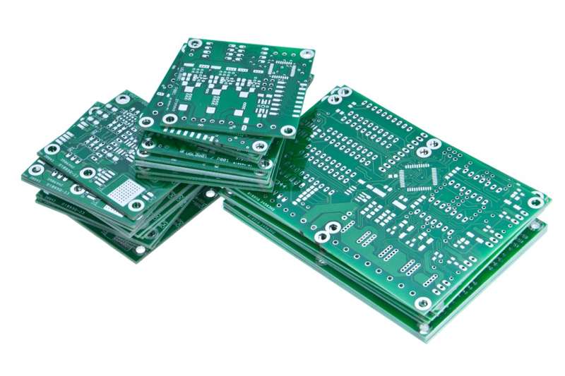
This unit is saddled with the responsibility of producing printed circuit boards of circuit designs which was handed to the unit by other Research and Development Units/Teams. A well designed schematic is critical to the overall Printed Circuit Board design process. Printed Circuit Board design is a two-stage process. First, the schematics of circuit designs is done using any of the various Computer Aided Design tools like the Easily Applicable Graphical Layout Editor (EAGLE), Proteus, Livewire etc. then a PCB layer is layed out based on these schematic designs. A thorough check for error and debugging is done before the final development of the Printed circuit board which involves the transfer of the layout onto copper clad board, etching of the unwanted area, then drilling and population of the board with the circuit‘s electronic components.
Unit Head : Engr. Benjamin Chinweze
Number Of Staff : -
KM 80 Enugu-Onitsha Express-way Awka Capital Territory PMB 5099
Awka, Anambra State, Nigeria.
© Copyright 2022 Electronics Development Institute - ELDI. All Rights Reserved
Created By ELDI ICT